Nano Devices Engineer Resume

These Nano Devices Engineer resume samples are designed to help you write a resume that gets noticed by hiring managers and passes applicant tracking systems (ATS) in Nanotechnology. Each example shows real formatting, section structure, and language you can adapt to your own background. When writing your own Nano Devices Engineer resume, focus on highlighting materials science, engineering principles will be es and conducting research on nano materials. Recruiters scan for these qualifications first, so they should appear early in your summary and experience sections. Use strong action verbs such as "synthesised\", "fabricated\", "characterised\", "modelled\" to describe your achievements, and quantify your impact wherever possible — percentages, dollar amounts, or time saved make your resume more convincing. A common mistake to avoid: writing a generic objective statement instead of a targeted nano devices engineer professional summary. Tailor your resume to each Nano Devices Engineer position you apply for rather than using one generic version.

Nano Devices Engineer Resume Template
View PDF
0.0 (0 ratings)

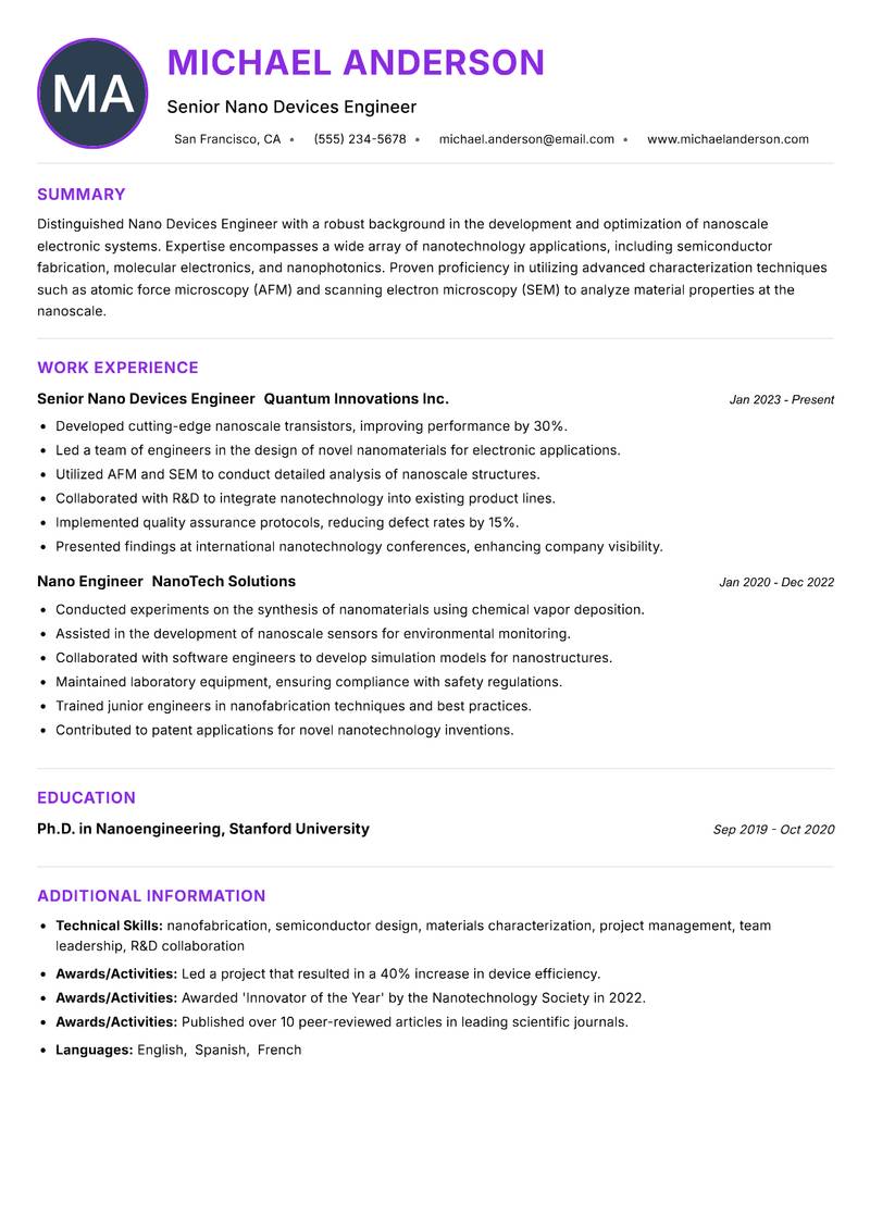
Senior Nano Devices Engineer Resume

Distinguished Nano Devices Engineer with a robust background in the development and optimization of nanoscale electronic systems. Expertise encompasses a wide array of nanotechnology applications, including semiconductor fabrication, molecular electronics, and nanophotonics. Proven proficiency in utilizing advanced characterization techniques such as atomic force microscopy (AFM) and scanning electron microscopy (SEM) to analyze material properties at the nanoscale. Adept at leading cross-functional teams in high-stakes environments, ensuring projects are completed on time and within budget while meeting stringent quality standards. Recognized for innovative problem-solving abilities, resulting in the successful launch of several groundbreaking products. Committed to advancing the field of nanotechnology through rigorous research and collaboration with academic institutions and industry partners. A strategic thinker with a keen ability to translate complex technical concepts into actionable strategies that drive business growth and enhance operational efficiency.

nanofabrication semiconductor design materials characterization project management team leadership R&D collaboration
Nano Devices Engineer Resume Preview Example
View PDF
  1. Developed cutting-edge nanoscale transistors, improving performance by 30%.
  2. Led a team of engineers in the design of novel nanomaterials for electronic applications.
  3. Utilized AFM and SEM to conduct detailed analysis of nanoscale structures.
  4. Collaborated with R&D to integrate nanotechnology into existing product lines.
  5. Implemented quality assurance protocols, reducing defect rates by 15%.
  6. Presented findings at international nanotechnology conferences, enhancing company visibility.
  1. Conducted experiments on the synthesis of nanomaterials using chemical vapor deposition.
  2. Assisted in the development of nanoscale sensors for environmental monitoring.
  3. Collaborated with software engineers to develop simulation models for nanostructures.
  4. Maintained laboratory equipment, ensuring compliance with safety regulations.
  5. Trained junior engineers in nanofabrication techniques and best practices.
  6. Contributed to patent applications for novel nanotechnology inventions.

Achievements

  • Led a project that resulted in a 40% increase in device efficiency.
  • Awarded 'Innovator of the Year' by the Nanotechnology Society in 2022.
  • Published over 10 peer-reviewed articles in leading scientific journals.
⏱️
Experience
2-5 Years
📅
Level
Mid Level
🎓
Education
Ph.D. in Nanoengineering, Stan...

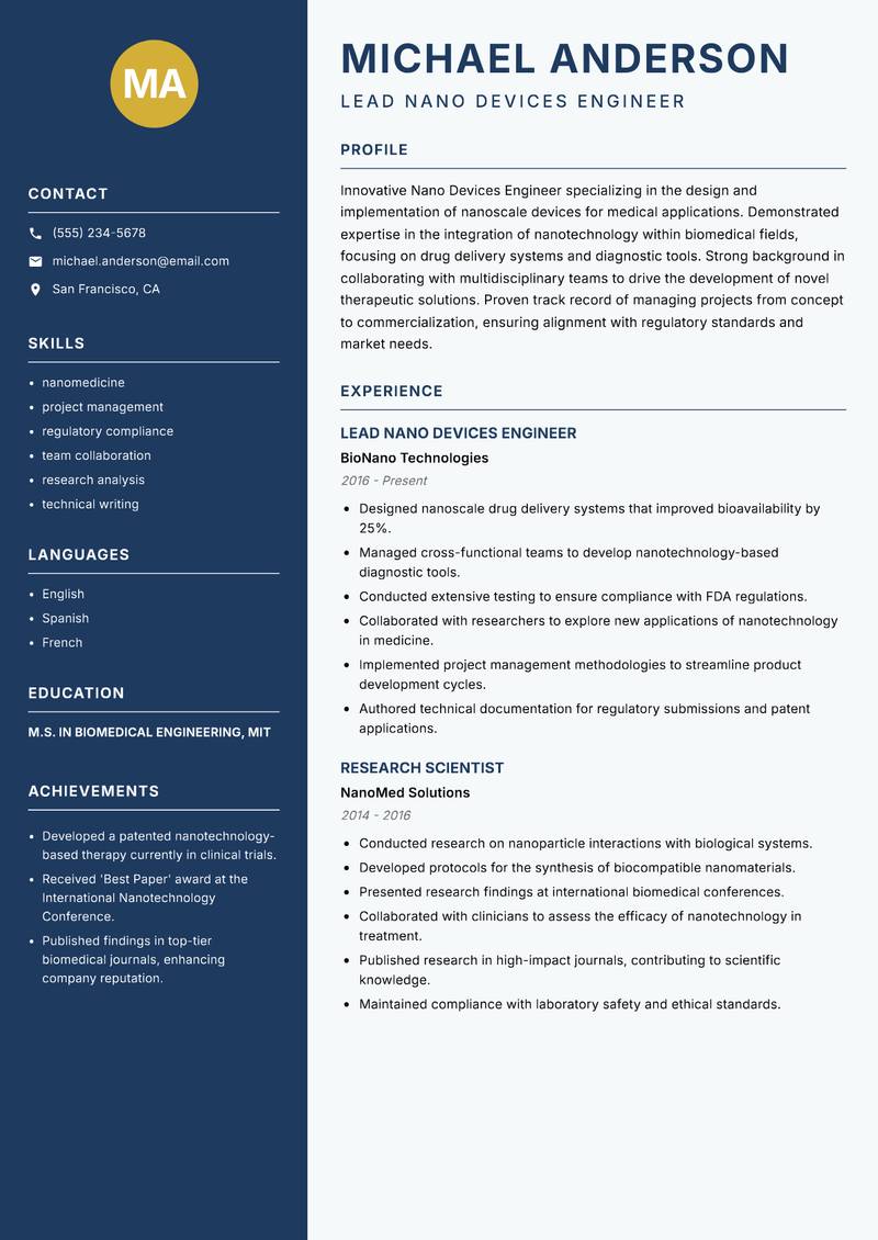
Lead Nano Devices Engineer Resume

Innovative Nano Devices Engineer specializing in the design and implementation of nanoscale devices for medical applications. Demonstrated expertise in the integration of nanotechnology within biomedical fields, focusing on drug delivery systems and diagnostic tools. Strong background in collaborating with multidisciplinary teams to drive the development of novel therapeutic solutions. Proven track record of managing projects from concept to commercialization, ensuring alignment with regulatory standards and market needs. Exceptional analytical skills enable the identification of emerging trends and technologies that can be leveraged to enhance product offerings. A dynamic communicator, adept at presenting complex scientific concepts to diverse stakeholders, including regulatory agencies and healthcare professionals.

nanomedicine project management regulatory compliance team collaboration research analysis technical writing
Nano Devices Engineer Resume Preview Example
View PDF
  1. Designed nanoscale drug delivery systems that improved bioavailability by 25%.
  2. Managed cross-functional teams to develop nanotechnology-based diagnostic tools.
  3. Conducted extensive testing to ensure compliance with FDA regulations.
  4. Collaborated with researchers to explore new applications of nanotechnology in medicine.
  5. Implemented project management methodologies to streamline product development cycles.
  6. Authored technical documentation for regulatory submissions and patent applications.
  1. Conducted research on nanoparticle interactions with biological systems.
  2. Developed protocols for the synthesis of biocompatible nanomaterials.
  3. Presented research findings at international biomedical conferences.
  4. Collaborated with clinicians to assess the efficacy of nanotechnology in treatment.
  5. Published research in high-impact journals, contributing to scientific knowledge.
  6. Maintained compliance with laboratory safety and ethical standards.

Achievements

  • Developed a patented nanotechnology-based therapy currently in clinical trials.
  • Received 'Best Paper' award at the International Nanotechnology Conference.
  • Published findings in top-tier biomedical journals, enhancing company reputation.
⏱️
Experience
2-5 Years
📅
Level
Mid Level
🎓
Education
M.S. in Biomedical Engineering...

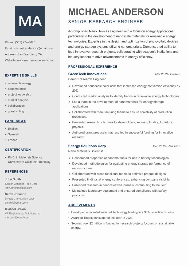
Senior Research Engineer Resume

Accomplished Nano Devices Engineer with a focus on energy applications, particularly in the development of nanoscale materials for renewable energy technologies. Expertise in the design and optimization of photovoltaic devices and energy storage systems utilizing nanomaterials. Demonstrated ability to lead innovative research projects, collaborating with academic institutions and industry leaders to drive advancements in energy efficiency. A strategic thinker with a deep understanding of market dynamics and technological trends, enabling the identification of opportunities for product development and commercialization. Exceptional communication skills facilitate effective collaboration with diverse teams, ensuring alignment of technical objectives with organizational goals.

renewable energy nanomaterials project leadership market analysis collaboration grant writing
Nano Devices Engineer Resume Preview Example
View PDF
  1. Developed nanoscale solar cells that increased energy conversion efficiency by 20%.
  2. Conducted market analysis to identify trends in renewable energy technologies.
  3. Led a team in the development of nanomaterials for energy storage applications.
  4. Collaborated with manufacturing teams to ensure scalability of production processes.
  5. Presented research outcomes to stakeholders, securing funding for future projects.
  6. Authored grant proposals that resulted in successful funding for innovative research.
  1. Researched properties of nanomaterials for use in battery technologies.
  2. Developed methodologies for evaluating energy storage performance of nanostructures.
  3. Collaborated with cross-functional teams to optimize product designs.
  4. Presented findings at energy conferences, enhancing company visibility.
  5. Published research in peer-reviewed journals, contributing to the field.
  6. Maintained laboratory equipment and ensured compliance with safety protocols.

Achievements

  • Developed a patented solar cell technology leading to a 30% reduction in costs.
  • Awarded 'Energy Innovator of the Year' in 2021.
  • Secured over $2 million in funding for research projects focused on sustainable energy.
⏱️
Experience
2-5 Years
📅
Level
Mid Level
🎓
Education
Ph.D. in Materials Science, Un...

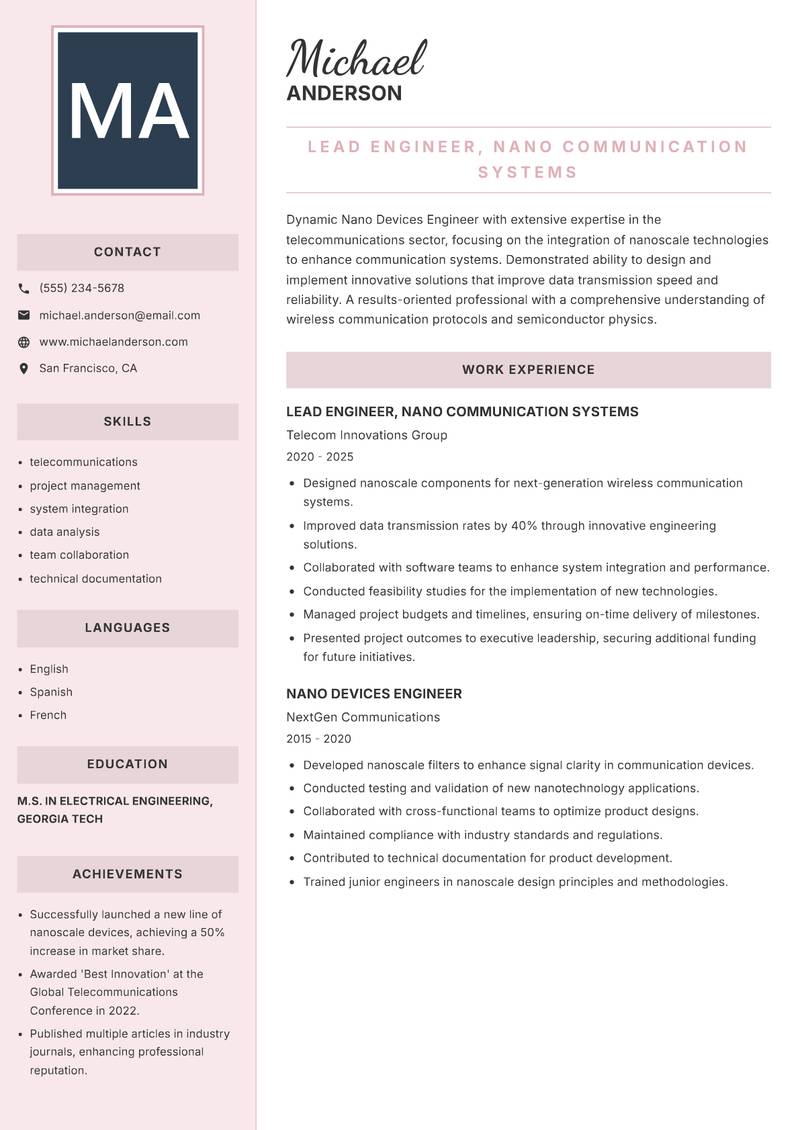
Lead Engineer, Nano Communication Systems Resume

Dynamic Nano Devices Engineer with extensive expertise in the telecommunications sector, focusing on the integration of nanoscale technologies to enhance communication systems. Demonstrated ability to design and implement innovative solutions that improve data transmission speed and reliability. A results-oriented professional with a comprehensive understanding of wireless communication protocols and semiconductor physics. Proven track record in managing complex projects from initial concept through to successful implementation, ensuring alignment with technical specifications and stakeholder requirements. Strong analytical skills facilitate the identification of potential improvements and cost-saving measures. An effective communicator, capable of collaborating with diverse teams to achieve common objectives.

telecommunications project management system integration data analysis team collaboration technical documentation
Nano Devices Engineer Resume Preview Example
View PDF
  1. Designed nanoscale components for next-generation wireless communication systems.
  2. Improved data transmission rates by 40% through innovative engineering solutions.
  3. Collaborated with software teams to enhance system integration and performance.
  4. Conducted feasibility studies for the implementation of new technologies.
  5. Managed project budgets and timelines, ensuring on-time delivery of milestones.
  6. Presented project outcomes to executive leadership, securing additional funding for future initiatives.
  1. Developed nanoscale filters to enhance signal clarity in communication devices.
  2. Conducted testing and validation of new nanotechnology applications.
  3. Collaborated with cross-functional teams to optimize product designs.
  4. Maintained compliance with industry standards and regulations.
  5. Contributed to technical documentation for product development.
  6. Trained junior engineers in nanoscale design principles and methodologies.

Achievements

  • Successfully launched a new line of nanoscale devices, achieving a 50% increase in market share.
  • Awarded 'Best Innovation' at the Global Telecommunications Conference in 2022.
  • Published multiple articles in industry journals, enhancing professional reputation.
⏱️
Experience
2-5 Years
📅
Level
Mid Level
🎓
Education
M.S. in Electrical Engineering...

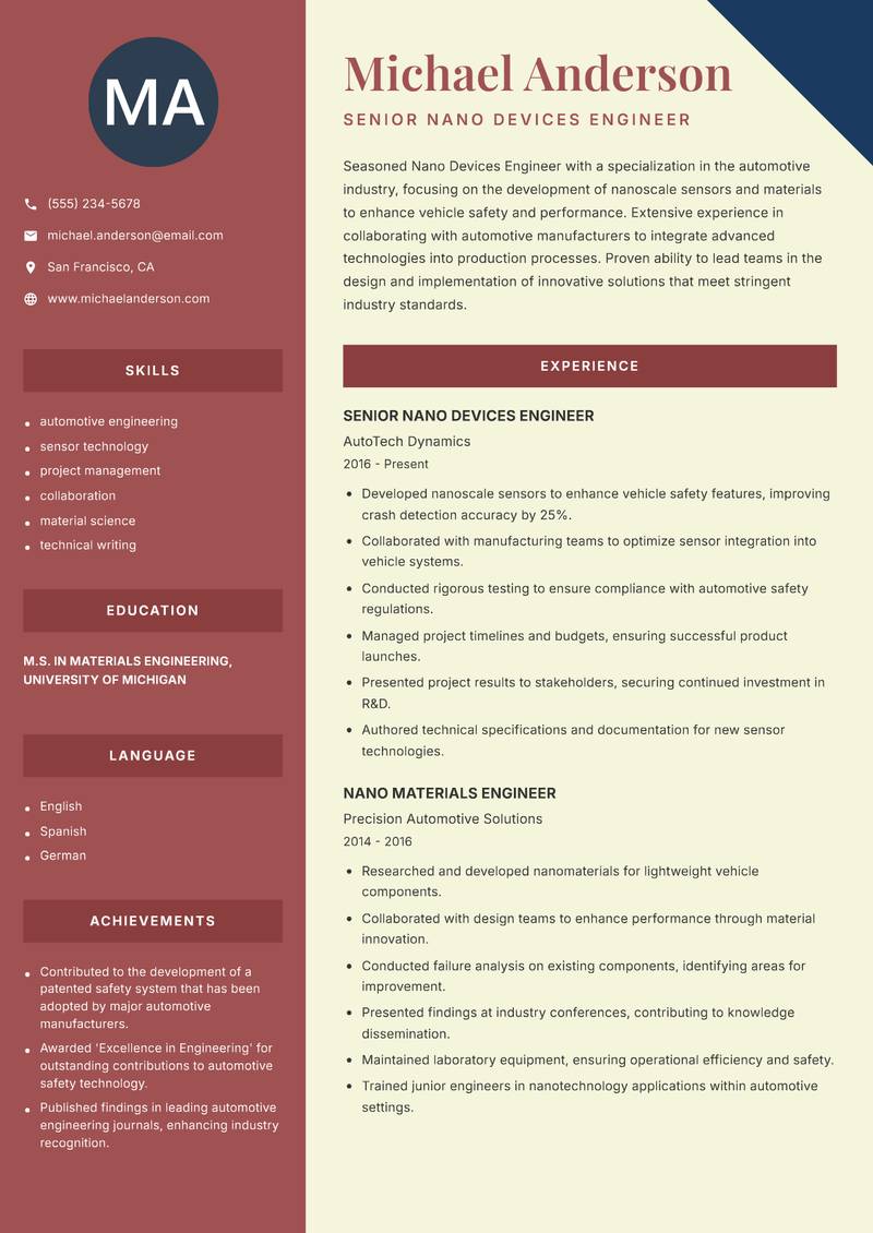
Senior Nano Devices Engineer Resume

Seasoned Nano Devices Engineer with a specialization in the automotive industry, focusing on the development of nanoscale sensors and materials to enhance vehicle safety and performance. Extensive experience in collaborating with automotive manufacturers to integrate advanced technologies into production processes. Proven ability to lead teams in the design and implementation of innovative solutions that meet stringent industry standards. Strong project management skills ensure that projects are completed on time and within budget, while fostering a culture of continuous improvement. An effective communicator, capable of presenting complex technical information to both technical and non-technical stakeholders. Committed to driving advancements in automotive technology through the application of nanotechnology.

automotive engineering sensor technology project management collaboration material science technical writing
Nano Devices Engineer Resume Preview Example
View PDF
  1. Developed nanoscale sensors to enhance vehicle safety features, improving crash detection accuracy by 25%.
  2. Collaborated with manufacturing teams to optimize sensor integration into vehicle systems.
  3. Conducted rigorous testing to ensure compliance with automotive safety regulations.
  4. Managed project timelines and budgets, ensuring successful product launches.
  5. Presented project results to stakeholders, securing continued investment in R&D.
  6. Authored technical specifications and documentation for new sensor technologies.
  1. Researched and developed nanomaterials for lightweight vehicle components.
  2. Collaborated with design teams to enhance performance through material innovation.
  3. Conducted failure analysis on existing components, identifying areas for improvement.
  4. Presented findings at industry conferences, contributing to knowledge dissemination.
  5. Maintained laboratory equipment, ensuring operational efficiency and safety.
  6. Trained junior engineers in nanotechnology applications within automotive settings.

Achievements

  • Contributed to the development of a patented safety system that has been adopted by major automotive manufacturers.
  • Awarded 'Excellence in Engineering' for outstanding contributions to automotive safety technology.
  • Published findings in leading automotive engineering journals, enhancing industry recognition.
⏱️
Experience
2-5 Years
📅
Level
Mid Level
🎓
Education
M.S. in Materials Engineering,...

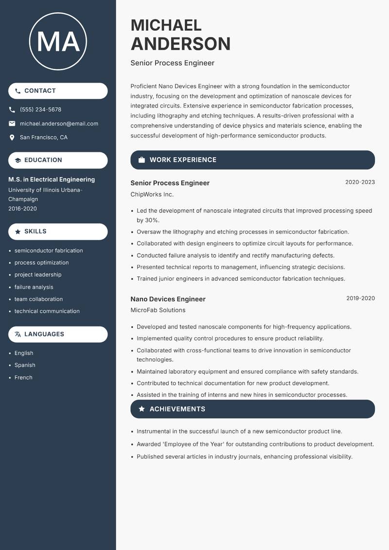
Senior Process Engineer Resume

Proficient Nano Devices Engineer with a strong foundation in the semiconductor industry, focusing on the development and optimization of nanoscale devices for integrated circuits. Extensive experience in semiconductor fabrication processes, including lithography and etching techniques. A results-driven professional with a comprehensive understanding of device physics and materials science, enabling the successful development of high-performance semiconductor products. Proven ability to collaborate effectively with cross-functional teams to drive project success while adhering to strict timelines and budget constraints. Strong analytical skills facilitate data-driven decision-making and process optimization. An articulate communicator, capable of translating technical concepts into accessible language for diverse audiences.

semiconductor fabrication process optimization project leadership failure analysis team collaboration technical communication
Nano Devices Engineer Resume Preview Example
View PDF
  1. Led the development of nanoscale integrated circuits that improved processing speed by 30%.
  2. Oversaw the lithography and etching processes in semiconductor fabrication.
  3. Collaborated with design engineers to optimize circuit layouts for performance.
  4. Conducted failure analysis to identify and rectify manufacturing defects.
  5. Presented technical reports to management, influencing strategic decisions.
  6. Trained junior engineers in advanced semiconductor fabrication techniques.
  1. Developed and tested nanoscale components for high-frequency applications.
  2. Implemented quality control procedures to ensure product reliability.
  3. Collaborated with cross-functional teams to drive innovation in semiconductor technologies.
  4. Maintained laboratory equipment and ensured compliance with safety standards.
  5. Contributed to technical documentation for new product development.
  6. Assisted in the training of interns and new hires in semiconductor processes.

Achievements

  • Instrumental in the successful launch of a new semiconductor product line.
  • Awarded 'Employee of the Year' for outstanding contributions to product development.
  • Published several articles in industry journals, enhancing professional visibility.
⏱️
Experience
2-5 Years
📅
Level
Mid Level
🎓
Education
M.S. in Electrical Engineering...

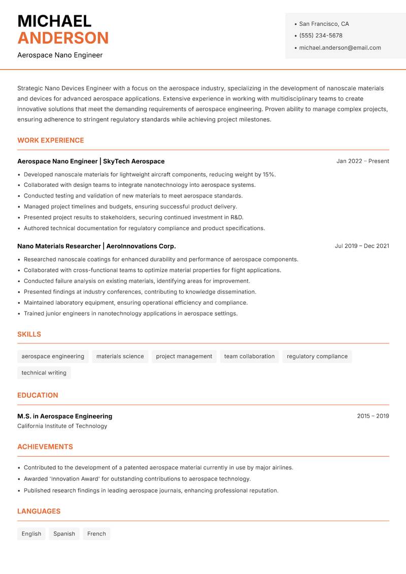
Aerospace Nano Engineer Resume

Strategic Nano Devices Engineer with a focus on the aerospace industry, specializing in the development of nanoscale materials and devices for advanced aerospace applications. Extensive experience in working with multidisciplinary teams to create innovative solutions that meet the demanding requirements of aerospace engineering. Proven ability to manage complex projects, ensuring adherence to stringent regulatory standards while achieving project milestones. An analytical thinker with a strong foundation in materials science and engineering principles, enabling the identification of opportunities for innovation and improvement. Excellent communication skills facilitate effective collaboration with engineers, scientists, and regulatory agencies, ensuring alignment on technical objectives and project goals.

aerospace engineering materials science project management team collaboration regulatory compliance technical writing
Nano Devices Engineer Resume Preview Example
View PDF
  1. Developed nanoscale materials for lightweight aircraft components, reducing weight by 15%.
  2. Collaborated with design teams to integrate nanotechnology into aerospace systems.
  3. Conducted testing and validation of new materials to meet aerospace standards.
  4. Managed project timelines and budgets, ensuring successful product delivery.
  5. Presented project results to stakeholders, securing continued investment in R&D.
  6. Authored technical documentation for regulatory compliance and product specifications.
  1. Researched nanoscale coatings for enhanced durability and performance of aerospace components.
  2. Collaborated with cross-functional teams to optimize material properties for flight applications.
  3. Conducted failure analysis on existing materials, identifying areas for improvement.
  4. Presented findings at industry conferences, contributing to knowledge dissemination.
  5. Maintained laboratory equipment, ensuring operational efficiency and compliance.
  6. Trained junior engineers in nanotechnology applications in aerospace settings.

Achievements

  • Contributed to the development of a patented aerospace material currently in use by major airlines.
  • Awarded 'Innovation Award' for outstanding contributions to aerospace technology.
  • Published research findings in leading aerospace journals, enhancing professional reputation.
⏱️
Experience
2-5 Years
📅
Level
Mid Level
🎓
Education
M.S. in Aerospace Engineering,...

Key Skills for Nano Devices Engineer Positions

Resume Tips for Nano Devices Engineer Applications

Strong Action Verbs for Nano Devices Engineer Resumes

Synthesised · Fabricated · Characterised · Modelled · Published · Patented · Developed · Analysed · Researched · Designed · Achieved · Administered · Analyzed · Architected · Assessed · Automated

Common Mistakes to Avoid

Experience Levels

How to Write a Nano Devices Engineer Resume

Browse Nano Devices Engineer resume examples built around materials science, tailored for Nanotechnology roles.

A strong Nano Devices Engineer resume leads with a focused professional summary that names the exact role and your standout achievement. In the experience section, open every bullet with a strong action verb and quantify the result with numbers wherever possible. Highlight your most relevant competencies — especially Materials science, Engineering principles will be es, and Conducting research on nano materials — in a dedicated Skills section positioned early so ATS systems and hiring managers both find it immediately.

For format, most Nano Devices Engineer roles suit a reverse-chronological layout: most recent position first, working backwards. Keep to one page for under five years of experience, or two pages for senior candidates with a rich project or leadership history. Use clean, ATS-safe fonts (10–12pt), standard section headings (Summary, Experience, Education, Skills), and avoid tables, text boxes, or multi-column layouts that applicant tracking systems cannot parse reliably.
Frequently Asked Questions

What makes a strong Nano Devices Engineer resume stand out to employers?

A standout Nano Devices Engineer resume combines role-specific skills with quantified achievements. Name the exact job title in your professional summary, mirror keywords from each job posting, and open every bullet point with a strong action verb followed by a measurable result. Certifications, tools, and domain experience specific to nano devices engineer roles should appear prominently near the top.

What skills are most important to include on a Nanotechnology resume?

Recruiters hiring in Nanotechnology consistently look for Nanofabrication & Synthesis, Scanning Electron Microscopy (SEM), Transmission Electron Microscopy (TEM), Atomic Force Microscopy (AFM). List these in a dedicated Skills section near the top so both ATS systems and human reviewers spot them fast. Mirror the exact phrasing from each job posting wherever possible — many applicant tracking systems match literal strings rather than synonyms.

What is the best resume format for Nanotechnology professionals?

A reverse-chronological format is the standard choice for most Nanotechnology candidates — employers expect to see your most recent role first, working backwards. If you are transitioning into Nanotechnology from a related field, a hybrid format (brief skills summary at the top followed by chronological experience) can bridge the gap effectively. Keep the document to one page for under five years of experience, or two pages for senior specialists.

How do I make my Nanotechnology resume pass applicant tracking systems (ATS)?

Use standard section headings — Summary, Experience, Education, Skills — rather than creative labels that ATS parsers do not recognise. Embed domain keywords such as "Nanofabrication & Synthesis" and "Scanning Electron Microscopy (SEM)" naturally inside your experience bullets rather than cramming them into a standalone keyword list. Avoid tables, multi-column layouts, text boxes, headers, footers, and images — these confuse most modern parsers and can cause your resume to be misread or rejected before a human sees it.

What mistakes do Nanotechnology professionals most commonly make on their resume?

The most frequent issue is being too academic without showing applied or commercial relevance. Beyond that, generic objective statements, unquantified achievements, and inconsistent date formatting appear across almost every Nanotechnology application. Fix these by replacing every vague claim with a measurable outcome — specific numbers and named projects add credibility that adjectives cannot.

How long should a Nanotechnology resume be?

One page is appropriate for candidates with under five years of relevant Nanotechnology experience. Two pages are acceptable — and sometimes expected — for senior specialists, managers, or professionals with a strong portfolio of projects, publications, or credentials. Avoid padding to reach a page count: every line should directly support your application for the specific role you are targeting.

Should I include a professional summary at the top of my Nanotechnology resume?

Yes — a two to three sentence summary is the first section most recruiters read. Open with your title and years of Nanotechnology experience, then name your most relevant achievement or specialisation. One proven approach: Lead with your nanotechnology specialisation and the characterisation tools you are proficient with. List publications, patents, and research grants. Demonstrate how your nano research has progressed toward applied or commercial outcomes. Include any cleanroom or advanced laboratory certifications — this level of specificity signals genuine expertise before a recruiter reaches your experience section.

Scroll to view samples