PCB Design Engineer Resume

These PCB Design Engineer resume samples are designed to help you write a resume that gets noticed by hiring managers and passes applicant tracking systems (ATS) in Electronics Engineering. Each example shows real formatting, section structure, and language you can adapt to your own background. When writing your own PCB Design Engineer resume, focus on highlighting PCB design, as a PCB design and analog & digital circuit design. Recruiters scan for these qualifications first, so they should appear early in your summary and experience sections. Use strong action verbs such as "designed", "simulated", "implemented", "verified" to describe your achievements, and quantify your impact wherever possible — percentages, dollar amounts, or time saved make your resume more convincing. A common mistake to avoid: writing a generic objective statement instead of a targeted pcb design engineer professional summary. Tailor your resume to each PCB Design Engineer position you apply for rather than using one generic version.

PCB Design Engineer Resume Template
View PDF
0.0 (0 ratings)

Senior PCB Design Engineer Resume

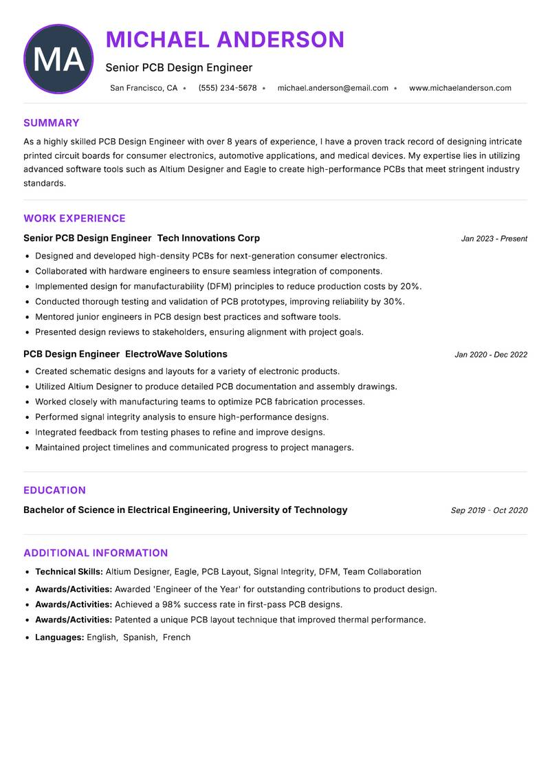
As a highly skilled PCB Design Engineer with over 8 years of experience, I have a proven track record of designing intricate printed circuit boards for consumer electronics, automotive applications, and medical devices. My expertise lies in utilizing advanced software tools such as Altium Designer and Eagle to create high-performance PCBs that meet stringent industry standards. I have successfully led projects from concept through production, ensuring that designs are optimized for manufacturability and reliability. My strong analytical skills enable me to troubleshoot complex issues, while my attention to detail ensures that every design is executed with precision. I am passionate about keeping up with the latest technology trends and continuously seek opportunities to enhance my skills. I thrive in collaborative environments and have effectively communicated with cross-functional teams to deliver projects on time and within budget. My commitment to quality and innovation in PCB design has consistently resulted in the successful launch of products that exceed customer expectations.

Altium Designer Eagle PCB Layout Signal Integrity DFM Team Collaboration
PCB Design Engineer Resume Preview Example
View PDF
  1. Designed and developed high-density PCBs for next-generation consumer electronics.
  2. Collaborated with hardware engineers to ensure seamless integration of components.
  3. Implemented design for manufacturability (DFM) principles to reduce production costs by 20%.
  4. Conducted thorough testing and validation of PCB prototypes, improving reliability by 30%.
  5. Mentored junior engineers in PCB design best practices and software tools.
  6. Presented design reviews to stakeholders, ensuring alignment with project goals.
  1. Created schematic designs and layouts for a variety of electronic products.
  2. Utilized Altium Designer to produce detailed PCB documentation and assembly drawings.
  3. Worked closely with manufacturing teams to optimize PCB fabrication processes.
  4. Performed signal integrity analysis to ensure high-performance designs.
  5. Integrated feedback from testing phases to refine and improve designs.
  6. Maintained project timelines and communicated progress to project managers.

Achievements

  • Awarded 'Engineer of the Year' for outstanding contributions to product design.
  • Achieved a 98% success rate in first-pass PCB designs.
  • Patented a unique PCB layout technique that improved thermal performance.
⏱️
Experience
2-5 Years
📅
Level
Mid Level
🎓
Education
Bachelor of Science in Electri...

PCB Design Engineer Resume

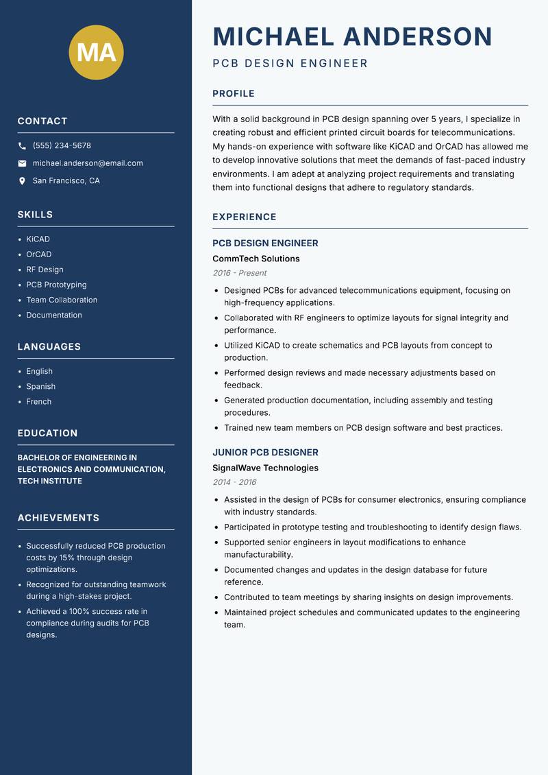
With a solid background in PCB design spanning over 5 years, I specialize in creating robust and efficient printed circuit boards for telecommunications. My hands-on experience with software like KiCAD and OrCAD has allowed me to develop innovative solutions that meet the demands of fast-paced industry environments. I am adept at analyzing project requirements and translating them into functional designs that adhere to regulatory standards. My role often involves collaboration with multidisciplinary teams to ensure that all aspects of the PCB design process are aligned with project goals. I am committed to continuous learning and regularly attend workshops to stay current with industry advancements. My analytical mindset and problem-solving abilities have been key in optimizing designs for performance and cost efficiency. As a PCB Design Engineer, I am passionate about contributing to the development of cutting-edge technologies that improve communication systems worldwide.

KiCAD OrCAD RF Design PCB Prototyping Team Collaboration Documentation
PCB Design Engineer Resume Preview Example
View PDF
  1. Designed PCBs for advanced telecommunications equipment, focusing on high-frequency applications.
  2. Collaborated with RF engineers to optimize layouts for signal integrity and performance.
  3. Utilized KiCAD to create schematics and PCB layouts from concept to production.
  4. Performed design reviews and made necessary adjustments based on feedback.
  5. Generated production documentation, including assembly and testing procedures.
  6. Trained new team members on PCB design software and best practices.
  1. Assisted in the design of PCBs for consumer electronics, ensuring compliance with industry standards.
  2. Participated in prototype testing and troubleshooting to identify design flaws.
  3. Supported senior engineers in layout modifications to enhance manufacturability.
  4. Documented changes and updates in the design database for future reference.
  5. Contributed to team meetings by sharing insights on design improvements.
  6. Maintained project schedules and communicated updates to the engineering team.

Achievements

  • Successfully reduced PCB production costs by 15% through design optimizations.
  • Recognized for outstanding teamwork during a high-stakes project.
  • Achieved a 100% success rate in compliance during audits for PCB designs.
⏱️
Experience
2-5 Years
📅
Level
Mid Level
🎓
Education
Bachelor of Engineering in Ele...

Lead PCB Design Engineer Resume

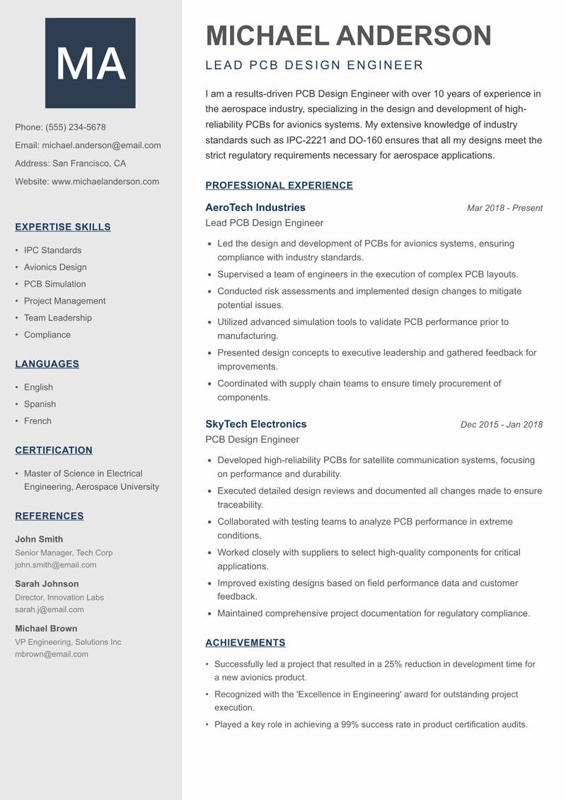
I am a results-driven PCB Design Engineer with over 10 years of experience in the aerospace industry, specializing in the design and development of high-reliability PCBs for avionics systems. My extensive knowledge of industry standards such as IPC-2221 and DO-160 ensures that all my designs meet the strict regulatory requirements necessary for aerospace applications. I have a passion for innovation and am always looking for ways to incorporate new technologies into my designs. My experience includes leading cross-functional teams through the entire product lifecycle, from initial concept to testing and production. I pride myself on my strong project management skills, which have enabled me to complete projects on time and within budget. My ability to communicate complex technical information to non-technical stakeholders has been instrumental in ensuring project alignment and success. I am committed to continuous improvement and actively seek feedback to enhance my design processes and outcomes.

IPC Standards Avionics Design PCB Simulation Project Management Team Leadership Compliance
PCB Design Engineer Resume Preview Example
View PDF
  1. Led the design and development of PCBs for avionics systems, ensuring compliance with industry standards.
  2. Supervised a team of engineers in the execution of complex PCB layouts.
  3. Conducted risk assessments and implemented design changes to mitigate potential issues.
  4. Utilized advanced simulation tools to validate PCB performance prior to manufacturing.
  5. Presented design concepts to executive leadership and gathered feedback for improvements.
  6. Coordinated with supply chain teams to ensure timely procurement of components.
  1. Developed high-reliability PCBs for satellite communication systems, focusing on performance and durability.
  2. Executed detailed design reviews and documented all changes made to ensure traceability.
  3. Collaborated with testing teams to analyze PCB performance in extreme conditions.
  4. Worked closely with suppliers to select high-quality components for critical applications.
  5. Improved existing designs based on field performance data and customer feedback.
  6. Maintained comprehensive project documentation for regulatory compliance.

Achievements

  • Successfully led a project that resulted in a 25% reduction in development time for a new avionics product.
  • Recognized with the 'Excellence in Engineering' award for outstanding project execution.
  • Played a key role in achieving a 99% success rate in product certification audits.
⏱️
Experience
2-5 Years
📅
Level
Mid Level
🎓
Education
Master of Science in Electrica...

PCB Design Engineer Resume

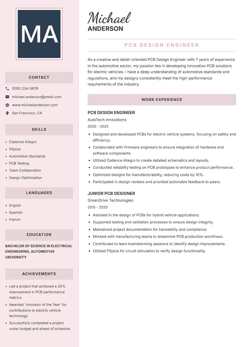
As a creative and detail-oriented PCB Design Engineer with 7 years of experience in the automotive sector, my passion lies in developing innovative PCB solutions for electric vehicles. I have a deep understanding of automotive standards and regulations, and my designs consistently meet the high-performance requirements of the industry. Proficient in using Cadence Allegro and PSpice, I have successfully contributed to several high-profile projects that focus on enhancing vehicle safety and performance. My collaborative approach allows me to work effectively with software and hardware teams to ensure that our designs are not only functional but also manufacturable. I am dedicated to professional development and actively seek opportunities to learn about emerging technologies in the automotive field. My commitment to quality and efficiency has led to the successful launch of multiple products, driving forward the future of mobility.

Cadence Allegro PSpice Automotive Standards PCB Testing Team Collaboration Design Optimization
PCB Design Engineer Resume Preview Example
View PDF
  1. Designed and developed PCBs for electric vehicle systems, focusing on safety and efficiency.
  2. Collaborated with firmware engineers to ensure integration of hardware and software components.
  3. Utilized Cadence Allegro to create detailed schematics and layouts.
  4. Conducted reliability testing on PCB prototypes to enhance product performance.
  5. Optimized designs for manufacturability, reducing costs by 10%.
  6. Participated in design reviews and provided actionable feedback to peers.
  1. Assisted in the design of PCBs for hybrid vehicle applications.
  2. Supported testing and validation processes to ensure design integrity.
  3. Maintained project documentation for traceability and compliance.
  4. Worked with manufacturing teams to streamline PCB production workflows.
  5. Contributed to team brainstorming sessions to identify design improvements.
  6. Utilized PSpice for circuit simulation to verify design functionality.

Achievements

  • Led a project that achieved a 30% improvement in PCB performance metrics.
  • Awarded 'Innovator of the Year' for contributions to electric vehicle technology.
  • Successfully completed a project under budget and ahead of schedule.
⏱️
Experience
2-5 Years
📅
Level
Mid Level
🎓
Education
Bachelor of Science in Electri...

Senior PCB Design Engineer Resume

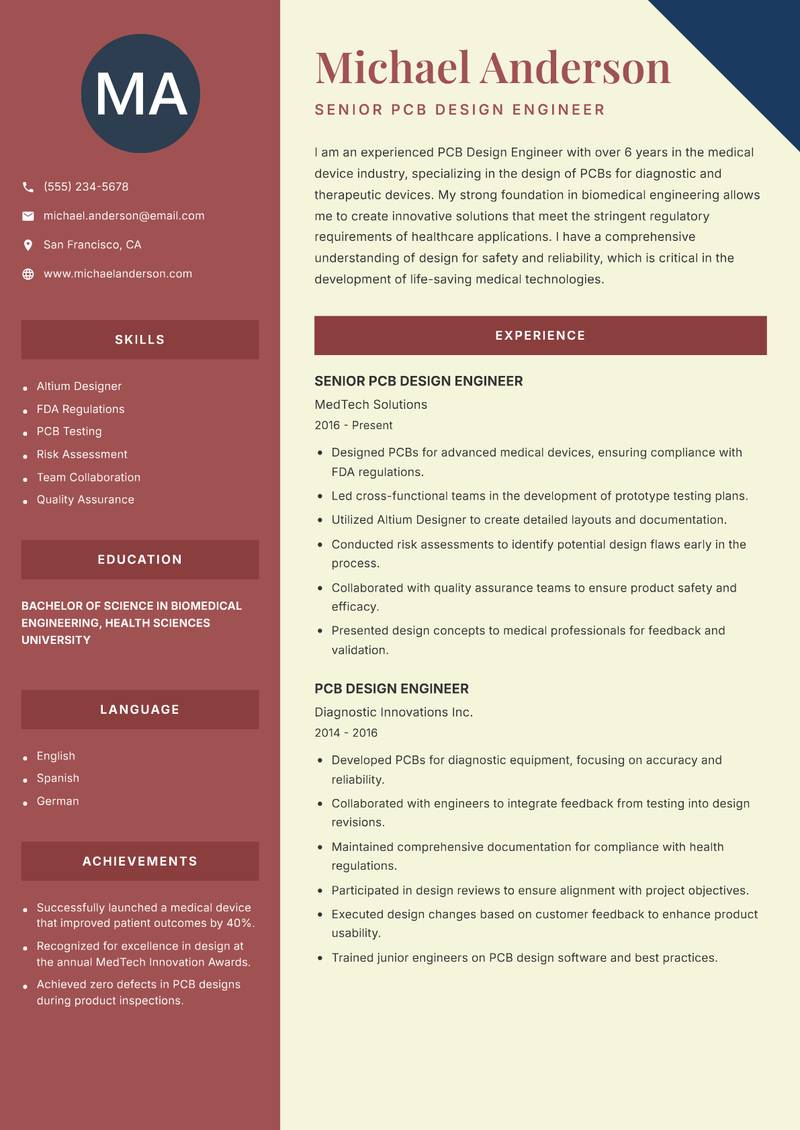
I am an experienced PCB Design Engineer with over 6 years in the medical device industry, specializing in the design of PCBs for diagnostic and therapeutic devices. My strong foundation in biomedical engineering allows me to create innovative solutions that meet the stringent regulatory requirements of healthcare applications. I have a comprehensive understanding of design for safety and reliability, which is critical in the development of life-saving medical technologies. I am proficient in using software such as Altium Designer and Mentor Graphics, and my designs have consistently resulted in successful product launches. My ability to communicate effectively with cross-functional teams ensures that all project requirements are met, and I am dedicated to maintaining high standards of quality throughout the design process. I am passionate about contributing to advancements in healthcare technology and am committed to continuous professional development.

Altium Designer FDA Regulations PCB Testing Risk Assessment Team Collaboration Quality Assurance
PCB Design Engineer Resume Preview Example
View PDF
  1. Designed PCBs for advanced medical devices, ensuring compliance with FDA regulations.
  2. Led cross-functional teams in the development of prototype testing plans.
  3. Utilized Altium Designer to create detailed layouts and documentation.
  4. Conducted risk assessments to identify potential design flaws early in the process.
  5. Collaborated with quality assurance teams to ensure product safety and efficacy.
  6. Presented design concepts to medical professionals for feedback and validation.
  1. Developed PCBs for diagnostic equipment, focusing on accuracy and reliability.
  2. Collaborated with engineers to integrate feedback from testing into design revisions.
  3. Maintained comprehensive documentation for compliance with health regulations.
  4. Participated in design reviews to ensure alignment with project objectives.
  5. Executed design changes based on customer feedback to enhance product usability.
  6. Trained junior engineers on PCB design software and best practices.

Achievements

  • Successfully launched a medical device that improved patient outcomes by 40%.
  • Recognized for excellence in design at the annual MedTech Innovation Awards.
  • Achieved zero defects in PCB designs during product inspections.
⏱️
Experience
2-5 Years
📅
Level
Mid Level
🎓
Education
Bachelor of Science in Biomedi...

PCB Design Engineer Resume

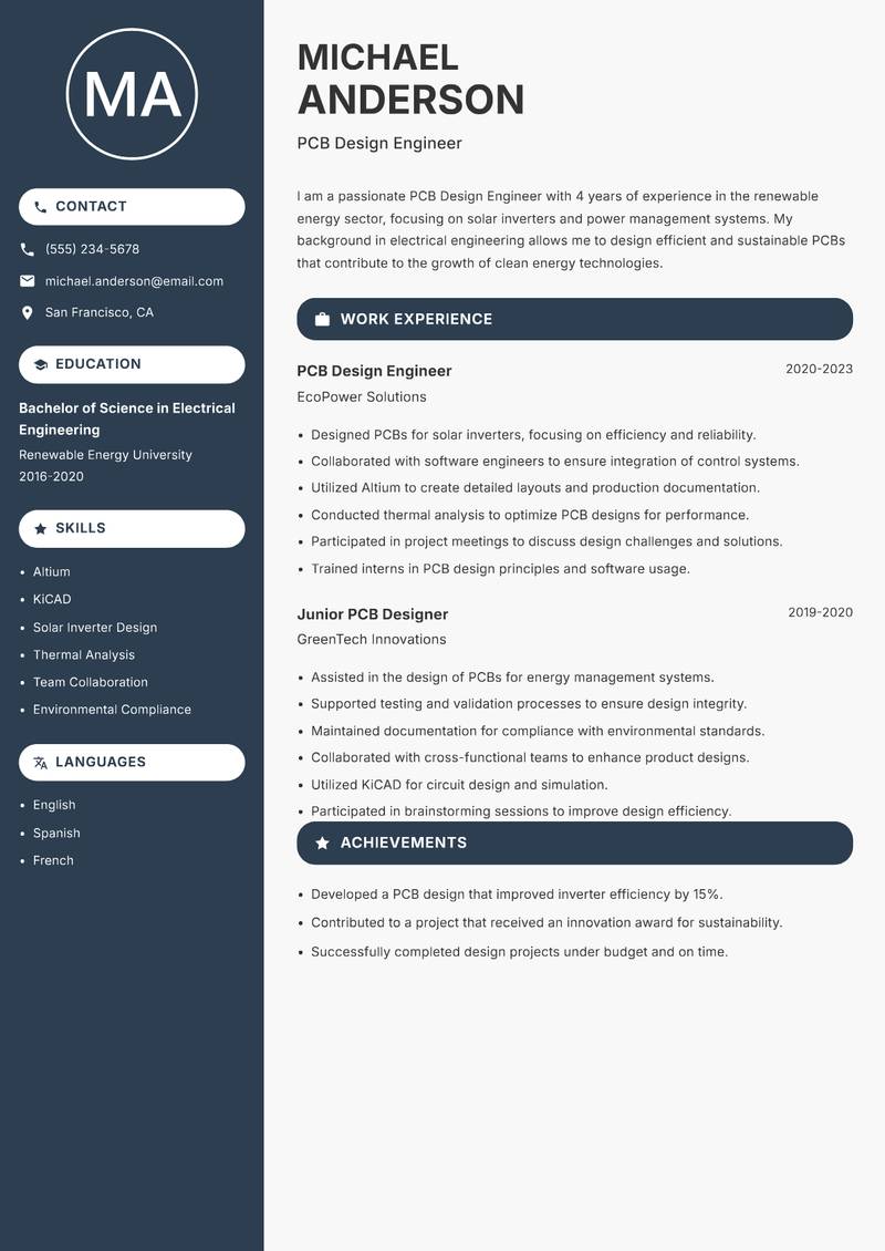
I am a passionate PCB Design Engineer with 4 years of experience in the renewable energy sector, focusing on solar inverters and power management systems. My background in electrical engineering allows me to design efficient and sustainable PCBs that contribute to the growth of clean energy technologies. I am skilled in using PCB design tools such as Altium and KiCAD, and I have a strong understanding of environmental regulations and standards. My approach to design emphasizes sustainability while ensuring performance and reliability. I thrive in collaborative environments and have a proven ability to communicate technical information to diverse audiences. I am committed to staying current with industry trends and continuously seek opportunities to improve my skills and knowledge in renewable energy technologies. My dedication to innovation has led to successful product developments that align with the global push for sustainable solutions.

Altium KiCAD Solar Inverter Design Thermal Analysis Team Collaboration Environmental Compliance
PCB Design Engineer Resume Preview Example
View PDF
  1. Designed PCBs for solar inverters, focusing on efficiency and reliability.
  2. Collaborated with software engineers to ensure integration of control systems.
  3. Utilized Altium to create detailed layouts and production documentation.
  4. Conducted thermal analysis to optimize PCB designs for performance.
  5. Participated in project meetings to discuss design challenges and solutions.
  6. Trained interns in PCB design principles and software usage.
  1. Assisted in the design of PCBs for energy management systems.
  2. Supported testing and validation processes to ensure design integrity.
  3. Maintained documentation for compliance with environmental standards.
  4. Collaborated with cross-functional teams to enhance product designs.
  5. Utilized KiCAD for circuit design and simulation.
  6. Participated in brainstorming sessions to improve design efficiency.

Achievements

  • Developed a PCB design that improved inverter efficiency by 15%.
  • Contributed to a project that received an innovation award for sustainability.
  • Successfully completed design projects under budget and on time.
⏱️
Experience
2-5 Years
📅
Level
Mid Level
🎓
Education
Bachelor of Science in Electri...

PCB Design Engineer Resume

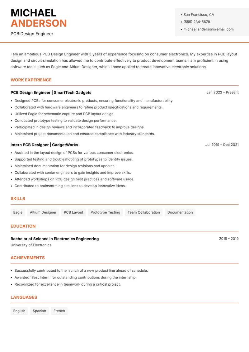
I am an ambitious PCB Design Engineer with 3 years of experience focusing on consumer electronics. My expertise in PCB layout design and circuit simulation has allowed me to contribute effectively to product development teams. I am proficient in using software tools such as Eagle and Altium Designer, which I have applied to create innovative electronic solutions. My approach emphasizes collaboration and communication, ensuring that I work closely with other engineers to meet project objectives. I have a strong understanding of the entire product lifecycle and am dedicated to producing high-quality designs that are both functional and manufacturable. I am eager to learn and grow in the field of electronics, and I consistently strive to enhance my technical skills and knowledge.

Eagle Altium Designer PCB Layout Prototype Testing Team Collaboration Documentation
PCB Design Engineer Resume Preview Example
View PDF
  1. Designed PCBs for consumer electronic products, ensuring functionality and manufacturability.
  2. Collaborated with hardware engineers to refine product specifications and requirements.
  3. Utilized Eagle for schematic capture and PCB layout design.
  4. Conducted prototype testing to validate design performance.
  5. Participated in design reviews and incorporated feedback to improve designs.
  6. Maintained project documentation and ensured compliance with industry standards.
  1. Assisted in the layout design of PCBs for various consumer electronics.
  2. Supported testing and troubleshooting of prototypes to identify issues.
  3. Maintained documentation for design revisions and updates.
  4. Collaborated with senior engineers to gain insights and improve skills.
  5. Attended workshops on PCB design best practices and software usage.
  6. Contributed to brainstorming sessions to develop innovative ideas.

Achievements

  • Successfully contributed to the launch of a new product line ahead of schedule.
  • Awarded 'Best Intern' for outstanding contributions during the internship.
  • Recognized for excellence in teamwork during a critical project.
⏱️
Experience
2-5 Years
📅
Level
Mid Level
🎓
Education
Bachelor of Science in Electro...

Key Skills for PCB Design Engineer Positions

Resume Tips for PCB Design Engineer Applications

Strong Action Verbs for PCB Design Engineer Resumes

Designed · Simulated · Implemented · Verified · Prototyped · Tested · Debugged · Optimized · Integrated · Deployed · Achieved · Administered · Analyzed · Architected

Common Mistakes to Avoid

Experience Levels

How to Write a PCB Design Engineer Resume

Browse PCB Design Engineer resume examples built around embedded C/C++ programming, tailored for Electronics Engineering roles.

A strong PCB Design Engineer resume leads with a focused professional summary that names the exact role and your standout achievement. In the experience section, open every bullet with a strong action verb and quantify the result with numbers wherever possible. Highlight your most relevant competencies — especially PCB Design, As a PCB Design, and Analog & Digital Circuit Design — in a dedicated Skills section positioned early so ATS systems and hiring managers both find it immediately.

For format, most PCB Design Engineer roles suit a reverse-chronological layout: most recent position first, working backwards. Keep to one page for under five years of experience, or two pages for senior candidates with a rich project or leadership history. Use clean, ATS-safe fonts (10–12pt), standard section headings (Summary, Experience, Education, Skills), and avoid tables, text boxes, or multi-column layouts that applicant tracking systems cannot parse reliably.
Frequently Asked Questions

What makes a strong PCB Design Engineer resume stand out to employers?

A standout PCB Design Engineer resume combines role-specific skills with quantified achievements. Name the exact job title in your professional summary, mirror keywords from each job posting, and open every bullet point with a strong action verb followed by a measurable result. Certifications, tools, and domain experience specific to pcb design engineer roles should appear prominently near the top.

What skills are most important to include on a Electronics Engineering resume?

Recruiters hiring in Electronics Engineering consistently look for Analog & Digital Circuit Design, PCB Layout & Signal Integrity, Embedded C/C++ Programming, FPGA Design (VHDL, Verilog). List these in a dedicated Skills section near the top so both ATS systems and human reviewers spot them fast. Mirror the exact phrasing from each job posting wherever possible — many applicant tracking systems match literal strings rather than synonyms.

What is the best resume format for Electronics Engineering professionals?

A reverse-chronological format is the standard choice for most Electronics Engineering candidates — employers expect to see your most recent role first, working backwards. If you are transitioning into Electronics Engineering from a related field, a hybrid format (brief skills summary at the top followed by chronological experience) can bridge the gap effectively. Keep the document to one page for under five years of experience, or two pages for senior specialists.

How do I make my Electronics Engineering resume pass applicant tracking systems (ATS)?

Use standard section headings — Summary, Experience, Education, Skills — rather than creative labels that ATS parsers do not recognise. Embed domain keywords such as "Analog & Digital Circuit Design" and "PCB Layout & Signal Integrity" naturally inside your experience bullets rather than cramming them into a standalone keyword list. Avoid tables, multi-column layouts, text boxes, headers, footers, and images — these confuse most modern parsers and can cause your resume to be misread or rejected before a human sees it.

What mistakes do Electronics Engineering professionals most commonly make on their resume?

The most frequent issue is not specifying EDA tools — electronics employers hire for tool-specific expertise. Beyond that, generic objective statements, unquantified achievements, and inconsistent date formatting appear across almost every Electronics Engineering application. Fix these by replacing every vague claim with a measurable outcome — specific numbers and named projects add credibility that adjectives cannot.

How long should a Electronics Engineering resume be?

One page is appropriate for candidates with under five years of relevant Electronics Engineering experience. Two pages are acceptable — and sometimes expected — for senior specialists, managers, or professionals with a strong portfolio of projects, publications, or credentials. Avoid padding to reach a page count: every line should directly support your application for the specific role you are targeting.

Should I include a professional summary at the top of my Electronics Engineering resume?

Yes — a two to three sentence summary is the first section most recruiters read. Open with your title and years of Electronics Engineering experience, then name your most relevant achievement or specialisation. One proven approach: List specific EDA tools: Altium Designer, Cadence Virtuoso, Mentor Graphics, OrCAD — this level of specificity signals genuine expertise before a recruiter reaches your experience section.

Scroll to view samples